Sometimes when you are creating PCB, you need to provide modularity or reconfiguration easily, e.g. creating connection between two or more points.
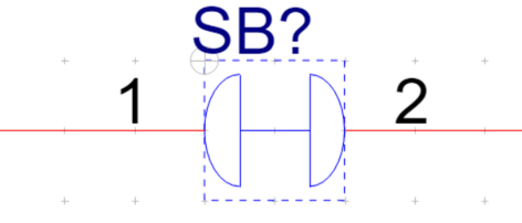
A solder bridge or solder jumpers is commonly used for this purpose and minimize the use of jumper resistors keeping simple the design, and could be short circuit (tin copper between both pads) or open circuit as below

Today I will show you how to do that in Cadense Allegro, I did it in Altium but in Cadense use a different method and is more complicated to be honest.
1. Firstly create a component symbol in capture for this particular “component”, i will use the short circuit as example.
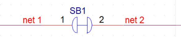
3. In properties for each pin include the name of the net you want to short circuit in this case, bet1 for pin 1 and net2 for pin2, as example below pin 1, do same for pin 2.


5. use your new symbol and foot print as you want :).
I hope this info help you, believe in Cadense is not easy to find this info easily and I decided to share this with my students.
This same methodology can be used in order to create net tie in Cadense.
have a nice day.